
News Release: Engineering the next generation of semiconductor materials, one layer at a time
July 1, 2026 — Silicon is an essential element for creating semiconductors, the building blocks of all modern-day computing technologies. However, as devices continue to shrink, engineers are approaching the limits of what silicon can achieve.
It’s time for some new materials.
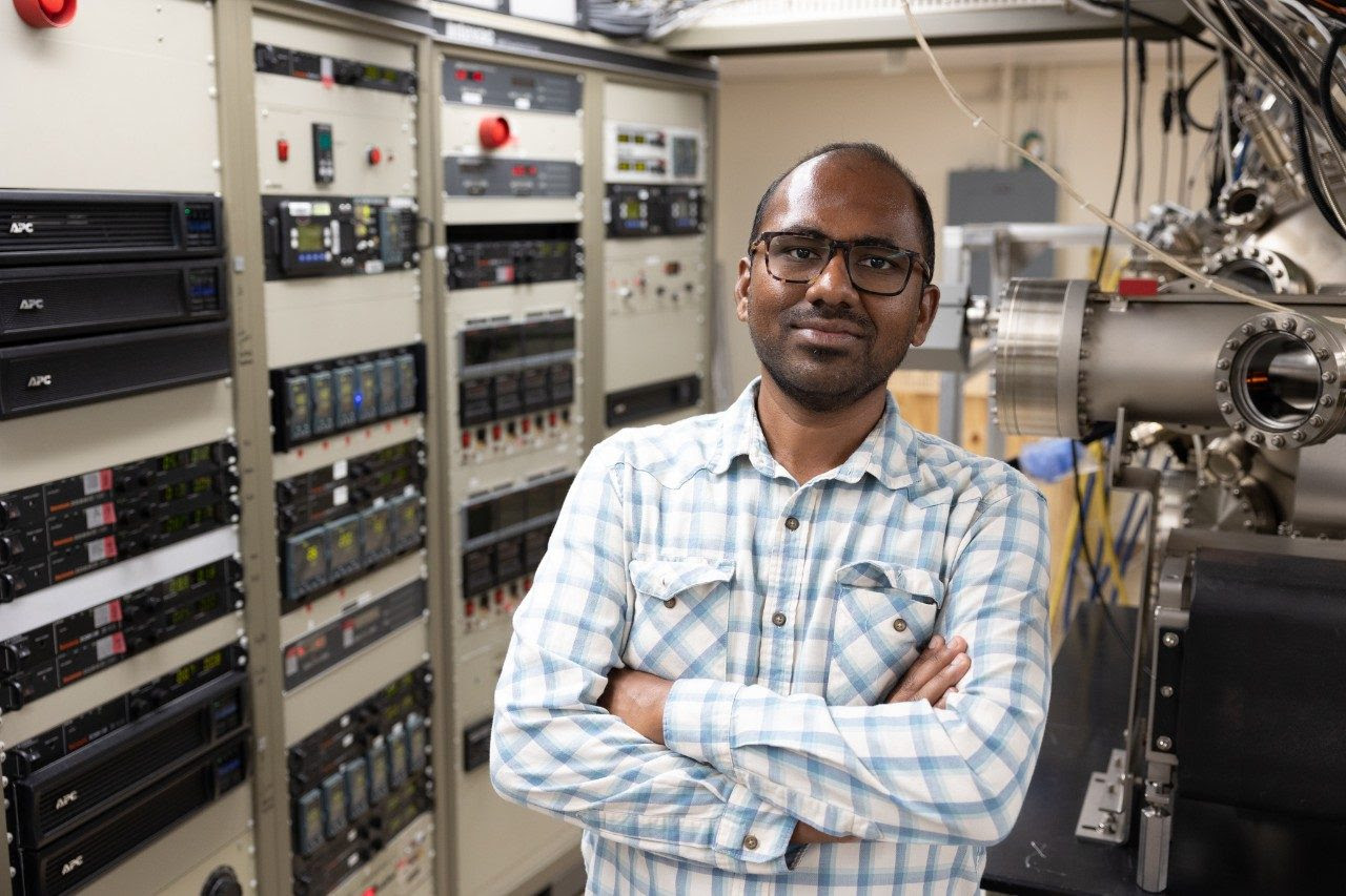
As a Ph.D. student in the Advanced Devices and Sustainable Energy Laboratory (ADSEL), Sengunthar Karthikeyan is helping to reinvent the foundation of semiconductors at the atomic level.
“The aim is to address the challenges in incorporating novel semiconductors in the future,” Karthikeyan said. “I’ve really enjoyed the hands-on research, growing material systems that have the potential to create different types of electronic and photonic devices, such as transistors, lasers, and photodetectors on the same platform.”
Creative solutions
Semiconductors are materials such as silicon with the ability to conduct or insulate against electricity. They serve as the microscopic on/off switches inside all modern electronics. As components have shrunk, engineers have encountered new challenges: electrons leaking through physical barriers in a process called tunneling and power density causing overheating. Silicon is also inefficient at emitting light, limiting its usefulness for photonic applications.
In the ADSEL group, Karthikeyan, his advisor Mantu Hudait, professor in the Bradley Department of Electrical and Computer Engineering, and fellow Ph.D. students experiment with elements such as indium, gallium, aluminum, tin, and germanium to create new materials that can replace silicon in future electronic systems. Components forged from new materials made from various combinations — such as indium-gallium-aluminum-
“ADSEL has given me an opportunity to analyze and understand the science behind the structure properties and co-relate them to device performance metrics,” said Karthikeyan. “I’ve been inspired to investigate numerous creative solutions before letting logistics interfere.”
For example, Karthikeyan spent nearly 14 hours carefully etching through a semiconductor layer to reach a target interface just nanometers thick. After missing the area on his first attempt, he repeated the experiment. He was able to successfully capture data used to characterize the material for future laser and photodetector applications. The efforts were detailed in his inaugural paper, Lattice‑matched GeSn with enhanced carrier confinement, published in the Journal of Materials Chemistry C.
What’s ahead
After completing his internship at Intel this summer, Karthikeyan will join the front end of line in the semiconductor industry, where he’s excited to bridge the gap between fundamental materials research and practical technology. His ultimate goal is to develop a way for transistors, lasers, and photodetectors to be manufactured together on the same semiconductor wafer.
“Karthikeyan’s contributions have strengthened our research in meaningful ways,” said Hudait. “His future impact will be significant. I’m excited to see him carry forward the curiosity, discipline, and integrity he has shown in our research group.”
Original study: DOI.10.1039/D3TC01018J